Shift Registers: Serial and Parallel Data Movement
Learning Objectives
By the end of this lesson, you should be able to:
- explain how a shift register stores and moves bits;
- compare SISO, SIPO, PISO, PIPO, and bidirectional shift registers;
- calculate latency, throughput, and pin savings;
- recognize common ICs such as 74HC595 and 74HC165;
- design simple serial-to-parallel and parallel-to-serial interfaces;
- debug clock, latch, load, and timing faults.
What Is a Shift Register?
A shift register is a chain of flip-flops that moves data one bit position on each clock edge.
Shift registers bridge serial and parallel worlds. They are used in UARTs, SPI peripherals, LED drivers, keyboard scanners, display interfaces, delay lines, ring counters, Johnson counters, CRC generators, and simple test-pattern hardware.
Naming Convention
The first word describes how data enters. The second word describes how data exits.
| Type | Input | Output | Main use |
|---|---|---|---|
| SISO | serial | serial | delay line |
| SIPO | serial | parallel | output expansion |
| PISO | parallel | serial | input reading |
| PIPO | parallel | parallel | register storage |
| bidirectional | serial or parallel | serial or parallel | flexible data movement |
Serial-In Serial-Out: SISO
SISO shifts one bit in and one bit out.

For an N-stage SISO register:
latency = N clock cycles
time delay = N / fclk
Example: a 16-bit SISO clocked at 1 MHz delays the first input bit by:
16 / 1,000,000 = 16 us
SISO State Example
Shifting 1011 into a 4-bit SISO initially cleared to 0000:
| Clock | Serial in | Q0 | Q1 | Q2 | Q3 |
|---|---|---|---|---|---|
| 0 | - | 0 | 0 | 0 | 0 |
| 1 | 1 | 1 | 0 | 0 | 0 |
| 2 | 0 | 0 | 1 | 0 | 0 |
| 3 | 1 | 1 | 0 | 1 | 0 |
| 4 | 1 | 1 | 1 | 0 | 1 |
The first input bit appears at the last stage after four clocks.
Serial-In Parallel-Out: SIPO
SIPO receives bits one at a time and presents the stored word on multiple output pins.
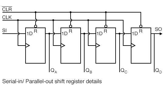
Common use: drive many LEDs using only data, clock, and latch pins.
For a 74HC595-style part:
- shift clock moves serial data through the internal register;
- latch clock copies the shifted word to output pins;
- output enable can tri-state the outputs;
- clear may reset the shift register.
SIPO Timing Sketch
title "SIPO shift then latch"
time start=0 end=80 unit=us divisions=8

DATA: square label="DATA bits" low=0 high=1 duty=50 cycles=4 unit=logic color=#2563eb
SHCP: square label="shift clock" low=0 high=1 duty=30 cycles=8 unit=logic color=#16a34a
STCP: pulse label="latch pulse" low=0 high=1 at=70 width=5 unit=logic color=#dc2626
marker LATCH at=70 label="outputs update"
The waveform is explanatory. Always use the datasheet setup, hold, and pulse-width values for a real IC.
Parallel-In Serial-Out: PISO
PISO loads many input bits at once, then shifts them out one bit at a time.

Common use: read many switches using only load, clock, and serial-data pins.
For a typical 74HC165:
- assert parallel load to capture all inputs;
- release load;
- apply clock pulses;
- read one serial bit per clock.
Parallel-In Parallel-Out: PIPO
PIPO is a regular parallel register. All input bits are captured together and all output bits are available together.

PIPO registers are used in CPUs, bus interfaces, FIFOs, pipeline stages, and temporary storage.
Bidirectional and Universal Shift Registers
A bidirectional register shifts left or right depending on a mode input. A universal shift register usually supports hold, shift left, shift right, and parallel load.
| S1 | S0 | Operation |
|---|---|---|
| 0 | 0 | hold |
| 0 | 1 | shift right |
| 1 | 0 | shift left |
| 1 | 1 | parallel load |

The 74HC194 is a classic 4-bit universal shift register.
Throughput and Latency
For a serial link that transfers one bit per shift clock:
bit_rate = fshift
time_to_transfer_N_bits = N / fshift
Example: send 24 LED bits to three cascaded 74HC595 devices at a 2 MHz shift clock.
transfer time = 24 / 2,000,000 = 12 us
The latch pulse can update all 24 outputs at once after shifting is complete.
Cascading Shift Registers
Shift registers can be cascaded by connecting serial output of one device to serial input of the next.
Design checks:
- the last bit shifted may appear at the farthest device first depending on bit order;
- all devices need the same clock and latch edges;
- long chains reduce maximum reliable speed;
- outputs should be latched only after all bits are shifted.
Ring, Johnson, and LFSR Uses
A ring counter recirculates a single 1:
0001 -> 0010 -> 0100 -> 1000 -> 0001
A Johnson counter feeds the inverted last bit back to the first bit:
0000 -> 0001 -> 0011 -> 0111 -> 1111 -> 1110 -> 1100 -> 1000 -> 0000
A linear feedback shift register, or LFSR, uses XOR feedback taps to generate a deterministic pseudo-random sequence. For an n-bit maximal LFSR:
sequence length = 2^n - 1
LFSRs are useful for CRCs, test patterns, scrambling, and lightweight pseudo-random sequences. They are not secure encryption by themselves.
Worked Example: Drive 16 LEDs With Three MCU Pins
Goal: control 16 LEDs from a microcontroller with limited GPIO.
Parts:
- two 74HC595 SIPO shift registers;
- 16 LED current-limit resistors;
- three MCU pins:
DATA,CLOCK,LATCH; - decoupling capacitor near each IC.
Connection plan:
MCU DATA  -> first 74HC595 SER
first QH' -> second 74HC595 SER
MCU CLOCK -> both SHCP pins
MCU LATCH -> both STCP pins
outputs   -> resistors -> LEDs
Expected behavior:
- shift 16 bits while latch is inactive;
- pulse latch once;
- all LEDs update together;
- changing data without clock does not move bits;
- shifting without latch does not change outputs on a latched device.
Minimal C-style pseudocode:
void shift16(uint16_t value) {
    for (int bit = 15; bit >= 0; bit--) {
        write_pin(DATA, (value >> bit) & 1);
        pulse_pin(CLOCK);
    }
    pulse_pin(LATCH);
}
Practical Verification
- Start with a slow clock, such as 1 Hz to 10 Hz, and observe LEDs.
- Shift a walking-one pattern:
0001,0010,0100, and so on. - Verify bit order by checking which output changes first.
- Confirm latch behavior separately from shift behavior.
- Check load polarity for PISO devices.
- Measure setup and hold timing when increasing speed.
- Add pull-ups or pull-downs to mechanical switch inputs.
Common Failure Symptoms
| Symptom | Likely cause | Debug action |
|---|---|---|
| outputs never change | latch not pulsed or output disabled | probe latch and OE pins |
| pattern appears reversed | wrong bit order | shift LSB-first or rewire output order |
| one-bit offset | extra or missing clock edge | count clock pulses with logic analyzer |
| random input readings | switch bounce or floating inputs | add pull resistors and debounce |
| works slow but not fast | setup/hold or wiring integrity issue | reduce speed, shorten wires, check datasheet |
| LEDs flicker during update | no output latch or latch pulsed too early | use latched register and update after shift |
Summary
Shift registers move bits between serial and parallel formats. SISO creates delay, SIPO expands outputs, PISO reads many inputs with few pins, PIPO stores a parallel word, and universal registers add flexible direction and load modes. Reliable designs depend on clock edges, latch/load polarity, setup/hold timing, and clear bit-order documentation.
Further Reading
- Datasheets for 74HC595, 74HC165, 74HC164, and 74HC194
- Texas Instruments, Logic Guide
- Microchip and ST application notes on GPIO expansion
- Stephen Brown and Zvonko Vranesic, Fundamentals of Digital Logic with Verilog Design